

NCERT Solutions for Class 12 Physics Chapter 14 - Semiconductor Electronic: Material, Devices And Simple Circuits
Related Chapters


1. In an n-type silicon, which of the following statements is true:
Electrons are majority carriers and trivalent atoms are the dopants.
Electrons are minority carriers and pentavalent atoms are the dopants.
Holes are minority carriers and pentavalent atoms are the dopants.
Holes are majority carriers and trivalent atoms are the dopants.
Ans: c) Electrons are majority carriers whereas holes are minority carriers in an n-type silicon atom.
When pentavalent atoms such as Phosphorus are doped in Silicon atoms, an n-type semiconductor is formed.
2. In an p-type silicon, which of the following statements is true:
Electrons are majority carriers and trivalent atoms are the dopants.
Electrons are minority carriers and pentavalent atoms are the dopants.
Holes are minority carriers and pentavalent atoms are the dopants.
Holes are majority carriers and trivalent atoms are the dopants.
Ans: d) Electrons are minority carriers whereas holes are majority carriers in an p-type silicon atom.
When trivalent atoms such as Aluminum are doped in Silicon atoms, an p-type semiconductor is formed.
3. Carbon, silicon and germanium have four valence electrons each. These are characterized by valence and conduction bands separated by energy band gap respectively equal to ${{({{E}_{g}})}_{C}}$, ${{({{E}_{g}})}_{Si}}$ and ${{({{E}_{g}})}_{Ge}}$ . Which of the following statements is true?
\[{{({{E}_{g}})}_{Si}}<{{({{E}_{g}})}_{Ge}}<{{({{E}_{g}})}_{C}}\]
\[{{({{E}_{g}})}_{C}}<{{({{E}_{g}})}_{Ge}}<{{({{E}_{g}})}_{Si}}\]
\[{{({{E}_{g}})}_{C}}>{{({{E}_{g}})}_{Si}}>{{({{E}_{g}})}_{Ge}}\]
\[{{({{E}_{g}})}_{C}}={{({{E}_{g}})}_{Si}}={{({{E}_{g}})}_{Ge}}\]
Ans: c) The energy band gap of Carbon is maximum and Germanium is minimum.
\[{{({{E}_{g}})}_{C}}>{{({{E}_{g}})}_{Si}}>{{({{E}_{g}})}_{Ge}}\] is the energy band gap order of Carbon, Silicon and Germanium.
4. In an unbiased p-n junction, holes diffuse from the p-region to n-region because
Free electrons in the n-region attract them.
They move across the junction by the potential difference.
Hole concentration in p-region is more as compared to n-region.
All the above
Ans: c) The concentration of holes is more in the p-type region than that of n-type region.
Diffusion of charge carriers takes place from the region of higher concentration to the region of lower concentration across a junction.
Therefore, in an unbiased p-n junction, holes diffuse from the p-type region to the n-type region.
5.When a forward bias is applied to a p-n junction, it
Raises the potential barrier.
Reduce the majority carrier current to zero.
Lower the potential barrier.
None of the above.
Ans: c) In forward bias of a p-n junction, the potential barrier is opposed by the applied voltage.
So, when forward bias is applied to a p-n junction, the potential barrier is lowered.
Therefore, the potential barrier across the junction decreases.
6. For transistor action, which of the following statements are correct.
Base, emitter and collector regions should have similar size and doping concentrations.
The base region must be very thin and lightly doped.
The emitter junction is forward biased and collector junction is reverse biased.
Both the emitter junction as well as the collector junction are forward biased.
Ans: (b) and (c) are correct statements.
The base region is lightly doped so that it is very thin whereas the emitter junction is forward biased and the collector junction is reverse biased for proper transistor action.
7. For a transistor amplifier, the voltage gain
Remains constant for all frequencies.
Is high at high and low frequencies and constant in the middle frequency range.
Is low at high and low frequencies and constant at mid frequencies.
None of the above.
Ans: c) In a transistor amplifier, the voltage gain is constant at the middle frequencies and low at both low and high frequencies.
8. In a half-wave rectifier, find the output frequency if the input frequency is \[~\mathbf{50Hz}\]. Also, find the output frequency of a full-wave rectifier for the same input frequency?
Ans: It is provided that,
Input frequency of rectifier$=50Hz$
It is known that,
The input frequency of a half-wave rectifier is equal to the output frequency.
$\Rightarrow $Output frequency$=50Hz$
The output frequency of a full-wave rectifier is twice the input frequency.
$\Rightarrow $Output frequency$=2\times 50=100Hz$
Therefore, the output frequency of a half-wave and full-wave rectifier with input frequency $50Hz$ is equal to $50Hz$and $100Hz$respectively.
9. For a CE-transistor amplifier, the audio signal voltage across the collector resistance of \[\mathbf{2}k\Omega \] is \[\mathbf{2}V\]Suppose the current amplification factor of the transistor is $100$, find the input signal voltage and base current, if the base resistance is \[1k\Omega \].
Ans: It is known that,
Voltage amplification, \[\frac{V}{{{V}_{i}}}=\beta \frac{{{R}_{c}}}{{{R}_{B}}}\]
Base resistance, ${{R}_{B}}=\frac{{{V}_{i}}}{{{V}_{B}}}$
It is given that for a CE-transistor amplifier,
Collector resistance, ${{R}_{c}}=2k\Omega =2000\Omega $
Audio signal voltage across the collector resistance, $V=2V$
Current amplification factor of the transistor, $\beta =100$$\Rightarrow $
Base resistance, \[{{R}_{b}}=1k\Omega =1000\Omega \]
Input signal voltage, ${{V}_{i}}=?$
Base current, ${{V}_{B}}=?$
From amplification relation: \[\frac{V}{{{V}_{i}}}=\beta \frac{{{R}_{c}}}{{{R}_{B}}}\]
$\Rightarrow \frac{2}{{{V}_{i}}}=100\times \frac{2000}{1000}$
$\Rightarrow \frac{2\times 1000}{100\times 2000}={{V}_{i}}$
$\Rightarrow {{V}_{i}}=\frac{1}{100}V$
$\Rightarrow {{V}_{i}}=0.01V$
From base resistance relation: ${{R}_{B}}=\frac{{{V}_{i}}}{{{V}_{B}}}$
$\Rightarrow {{R}_{B}}=\frac{0.01}{1000}$
$\Rightarrow {{R}_{B}}={{10}^{-6}}A=1\mu A$
Clearly, input signal voltage is $0.01V$and base current is $10\mu A$ for the given CE-transistor amplifier.
10. Two amplifiers are connected one after the other in series (cascaded). The first amplifier has a voltage gain of $10$ and the second has a voltage gain of $20$. If the input signal is $0.01$ volt, calculate the output ac signal.
Ans: It is given that,
Voltage gain of the first amplifier, ${{V}_{1}}=10$
Voltage gain of the second amplifier, ${{V}_{2}}=20$
Input signal voltage, ${{V}_{i}}=0.01V$
Output signal voltage, ${{V}_{o}}=?$
When two amplifiers are connected one after another is series (cascaded) the total voltage gain is the product of voltage gains of both amplifiers.
$\Rightarrow V={{V}_{1}}\times {{V}_{2}}$
$\Rightarrow V=10\times 20$
$\Rightarrow V=200$
Voltage amplification, $V=\frac{{{V}_{o}}}{{{V}_{i}}}$
$\Rightarrow 200=\frac{{{V}_{o}}}{0.01}$
$\Rightarrow {{V}_{o}}=200\times 0.01$
$\Rightarrow {{V}_{o}}=2V$
Thus, the output AC signal for the given amplifier is $2V$.
11. A p-n photodiode is fabricated from a semiconductor with a band gap of \[\mathbf{2}.\mathbf{8}\text{ }\mathbf{eV}\]. Can it detect a wavelength of \[\mathbf{6000}\text{ }\mathbf{nm}\]?
Ans: It is provided that,
Band gap of the p-n photodiode$=2.8eV$
Wavelength, $\lambda =6000nm=6\times {{10}^{-6}}m$
It is known that,
Energy of a signal, $E=\frac{hc}{\lambda }$
where,
$h$ is the Planck’s constant, $h=6.626\times {{10}^{-34}}Js$
$c$ is the speed of light, $c=3\times {{10}^{8}}m{{s}^{-1}}$
$\Rightarrow E=\frac{6.626\times {{10}^{-34}}\times 3\times {{10}^{8}}}{6\times {{10}^{-6}}}$
$\Rightarrow E=3.313\times {{10}^{-34+8+6}}$
$\Rightarrow E=3.313\times {{10}^{-20}}J$
It is known that, $1.6\times {{10}^{-19}}J=1eV$
$\Rightarrow E=\frac{3.313\times {{10}^{-20}}}{1.6\times {{10}^{-19}}}eV$
$\Rightarrow E=0.207eV$
Energy of the signal with wavelength $6000nm$is $0.207eV$.
As the energy of the signal is less than $2.8eV$(energy band gap of p-n photodiodes) the signal can’t be detected.
Therefore, the photodiode cannot detect the signal.
12. The number of silicon atoms per ${{m}^{3}}$ is $5\times {{10}^{28}}$. This is doped simultaneously with $5\times {{10}^{22}}$ atoms per ${{m}^{3}}$ of Arsenic and $5\times {{10}^{20}}$ per ${{m}^{3}}$ atoms of indium. Calculate the number of electrons and holes. Given that${{n}_{i}}=1.5\times {{10}^{16}}{{m}^{-3}}$. Is the material n-type or p-type?
Ans: It is provided that,
Number of silicon atoms, $N=5\times {{10}^{28}}atoms/{{m}^{3}}$
Number of arsenic atoms, ${{n}_{As}}=5\times {{10}^{22}}atoms/{{m}^{3}}$
Number of indium atoms, ${{n}_{In}}=5\times {{10}^{20}}atoms/{{m}^{3}}$
Number of thermally-generated electrons, ${{n}_{i}}=1.5\times {{10}^{16}}electrons/{{m}^{3}}$
Total number of electrons, ${{n}_{e}}={{n}_{As}}-{{n}_{i}}$
$\Rightarrow {{n}_{e}}=5\times {{10}^{22}}-1.5\times {{10}^{16}}$
$\Rightarrow {{n}_{e}}=(5-1.5\times {{10}^{-6}})\times {{10}^{22}}$
$\Rightarrow {{n}_{e}}\approx 4.99\times {{10}^{22}}electrons/{{m}^{3}}$
Number of holes, ${{n}_{h}}=?$
The concentration of electrons and holes in a semiconductor in thermal equilibrium is ${{n}_{e}}{{n}_{h}}={{n}_{i}}^{2}$
$\Rightarrow {{n}_{h}}=\frac{{{n}_{i}}^{2}}{{{n}_{e}}}$
$\Rightarrow {{n}_{h}}=\frac{{{(1.5\times {{10}^{16}})}^{2}}}{4.99\times {{10}^{22}}}$
$\Rightarrow {{n}_{h}}\approx 4.51\times {{10}^{9}}electrons/{{m}^{3}}$
Hence, the number of electrons is approximately equal to $4.99\times {{10}^{22}}$ electrons per ${{m}^{3}}$ and the number of holes is approximately equal to $4.51\times {{10}^{9}}$ electrons per ${{m}^{3}}$.
As the number of electrons is greater than the number of holes, the material is n-type semiconductor.
13. In an intrinsic semiconductor the energy gap ${{E}_{g}}$ is \[1.2\text{ }eV\]. Its hole mobility is much smaller than electron mobility and independent of temperature. What is the ratio between conductivity at \[600K\] and that at $300K$? Assume that the temperature dependence of intrinsic carrier concentration ${{n}_{i}}$ is given by ${{n}_{i}}={{n}_{o}}\exp \left( -\frac{{{E}_{g}}}{2{{k}_{B}}T} \right)$.
Ans: It is provided that,
Energy gap of the intrinsic semiconductor, ${{E}_{g}}=1.2eV$
Initial temperature, ${{T}_{1}}=300K$
Final temperature, ${{T}_{2}}=600K$
It is known that,
The temperature dependence of intrinsic carrier-concentration is:${{n}_{i}}={{n}_{o}}\exp \left( -\frac{{{E}_{g}}}{2{{k}_{B}}T} \right)$
Where,
${{k}_{B}}$ is the Boltzmann constant, ${{k}_{B}}=8.62\times {{10}^{-5}}eV/K$
$T$ is the Temperature
${{n}_{o}}$ is the constant
The intrinsic carrier-concentration at temperature ${{T}_{1}}=300K$: ${{n}_{i1}}={{n}_{o}}\exp \left( -\frac{{{E}_{g}}}{2{{k}_{B}}\times 300} \right)$
The intrinsic carrier-concentration at temperature ${{T}_{2}}=600K$:${{n}_{i2}}={{n}_{o}}\exp \left( -\frac{{{E}_{g}}}{2{{k}_{B}}\times 600} \right)$
Ratio between conductivities at $600K$ and $300K$is equal to the ratio between their respective intrinsic carrier- concentrations.
\[\Rightarrow \frac{{{n}_{i2}}}{{{n}_{i1}}}=\frac{{{n}_{o}}\exp \left( -\frac{{{E}_{g}}}{2{{k}_{B}}\times 600} \right)}{{{n}_{o}}\exp \left( -\frac{{{E}_{g}}}{2{{k}_{B}}\times 100} \right)}\]
$\Rightarrow \frac{{{n}_{i1}}}{{{n}_{i2}}}=\exp \frac{{{E}_{g}}}{2{{k}_{B}}}\left( \frac{1}{300}-\frac{1}{600} \right)$
$\Rightarrow \frac{{{n}_{i1}}}{{{n}_{i2}}}=\exp \frac{1.2}{2\times 8.62\times {{10}^{-5}}}\left( \frac{2-1}{600} \right)$
$\Rightarrow \frac{{{n}_{i1}}}{{{n}_{i2}}}=\exp (11.6)$
$\Rightarrow \frac{{{n}_{i1}}}{{{n}_{i2}}}=1.09\times {{10}^{5}}$
Thus, the ratio between the conductivities at $600K$ and $300K$ is $1.09\times {{10}^{5}}$.
14. In a p-n junction diode, the current $I$ can be expressed as $I={{I}_{0}}\exp \left( \left( \frac{eV}{{{k}_{B}}T} \right)-1 \right)$ where ${{I}_{0}}$ is called the reverse saturation current, $V$ is the voltage across the diode and is positive for forward bias and negative bias, and $I$ is the current through the diode, ${{k}_{B}}$ is the Boltzmann constant $(8.62\times {{10}^{-5}}eV/K)$ and $T$ is the absolute temperature. If for a given diode ${{I}_{0}}=5\times {{10}^{-12}}A$and\[\mathbf{T}\text{ }=\mathbf{300}\text{ }\mathbf{K}\], then
(a) What will be the forward current at a forward voltage of \[\mathbf{0}.\mathbf{6}\text{ }\mathbf{V}\]?
Ans: It is provided that,
Forward voltage, $V=0.6V$
Reverse saturation current, ${{I}_{0}}=5\times {{10}^{-12}}A$
Absolute temperature, $T=300K$
Boltzmann constant, ${{k}_{B}}=8.62\times {{10}^{-5}}eV/K$
It is known that,
Current in p-n junction diode is $I={{I}_{0}}\exp \left( \left( \frac{eV}{{{k}_{B}}T} \right)-1 \right)$
$\Rightarrow I=5\times {{10}^{-12}}\exp \left( \left( \frac{0.6}{8.62\times {{10}^{-5}}\times 300} \right)-1 \right)$
$\Rightarrow I=5\times {{10}^{-12}}\times \exp (22.36)$
$\Rightarrow I=0.0256A$
Therefore, the forward current is $0.0256A$.
(b)What will be the increase in the current if the voltage across the diode is increased to \[\mathbf{0}.\mathbf{7}\text{ }\mathbf{V}\]?
Ans: It is provided that,
Forward voltage, $V=0.7V$
Current in p-n junction diode is $I={{I}_{0}}\exp \left( \left( \frac{eV}{{{k}_{B}}T} \right)-1 \right)$
$\Rightarrow I=5\times {{10}^{-12}}\exp \left( \left( \frac{0.7}{8.62\times {{10}^{-5}}\times 300} \right)-1 \right)$
$\Rightarrow I=5\times {{10}^{-12}}\times \exp (26.25)$
$\Rightarrow I=1.257A$
Increase in current, $\Delta I=1.2757-0.0256$
$\Rightarrow \Delta I=1.23A$
Therefore, the increase in current $\Delta I=1.23A$
(C) What is dynamic resistance?
Ans: It is known that,
Dynamic resistance$=\frac{Change\text{ }in\text{ }voltage}{Change\text{ }in\text{ }current}$
$\Rightarrow \frac{(0.7-0.6)}{2.972}=0.0336/\Omega $
Therefore, the dynamic resistance is$0.0336/\Omega $.
(d) What will be the current if reverse bias voltage changes from \[\mathbf{1V}\] to \[2\mathbf{V}\]?
Ans: When reverse bias voltage changes from $1V$ to $2V$, the current$(I)$ remains almost equal to ${{I}_{0}}$ in both the cases. Change in current becomes equal to zero giving dynamic resistance an infinite value.
Hence, the dynamic resistance in the reverse bias would be infinite.
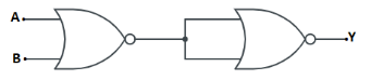
15. You are given the two circuits as shown in figure. Show that current
acts as OR gate
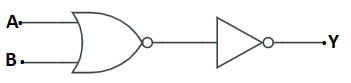
Ans: Inputs are A and B and Outputs are Y for the given circuit.
The first half of the figure represents NOR Gate and the right half represents NOT Gate.
From the figure, the output of the NOR gate is $\overline{A+B}$. This becomes the input of the NOT gate and its output becomes $\overline{\overline{A+B}}=A+B$.
The output of the system $Y=A+B$.
Therefore, the circuit functions as an OR gate.
(b) acts as AND gate
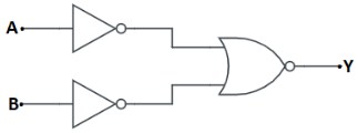
Ans: Inputs are A and B and output is Y for the given circuit.
The first half of the figure contains two NOT gates and the right half represents NOR Gate.
From the figure, the output of the circuit can be written as:
$Y=\overline{\overline{A}+\overline{B}}=\overline{\overline{A}}.\overline{\overline{B}}=A.B$
Therefore, the circuit functions as an AND gate.
16. Write the truth table for a NAND Gate connected as given in figure.
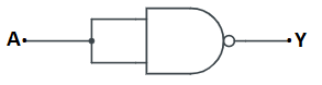
Hence identify the exact logic operation carried out by this circuit.
Ans: The input of the NAND gate is A and output is Y.
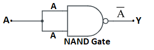
The output can be written as:
$Y=\overline{A.A}=\overline{A}+\overline{A}=\overline{A}$
Truth table for the given combination:
The symbol of the circuit:
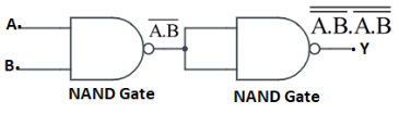
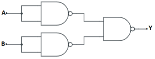
17. You are given two circuits as shown in figure, which consist of NAND gates. Identify the logic operation carried out by the two circuits.
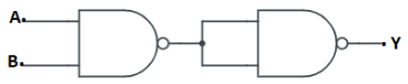
Ans: In the given circuit, inputs are A and B and output is Y.
The output of the left NAND gate is $\overline{A.B}$.
The output of the combination can be written as:
\[Y=\overline{(\overline{A.B}).(\overline{A.B})}=\overline{\overline{AB}}+\overline{\overline{AB}}=AB\]
Therefore, the circuit functions as an AND gate.
b)
Ans: In the given circuits, inputs are A and B and output is Y.
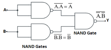
$\overline{A}$ is the output of the upper left NAND gate and $\overline{B}$ is the output of the lower left NAND gate.
The output of the combination can be written as:
$Y=\overline{A}.\overline{B}=\overline{\overline{A}}+\overline{\overline{B}}=A+B$
Therefore, the circuit acts as an OR gate.
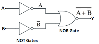
18. Write the truth table for circuit given in figure below consisting of NOR gates and identify the logic operation (OR, AND, NOT) which this circuit is performing.
(Hint:$A=0$, $B=1$ then A and B inputs of second NOR gate will be 0 and hence $Y=1$. Similarly work out the values of Y for other combinations of A and B. Compare with the truth table of OR, AND, NOT gates and find the correct one.)
Ans: The inputs of the AND gate are A and B.
The output of the first NOR gate is $\overline{A+B}$.
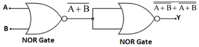
The output of the combination can be written as:
\[Y=\overline{\overline{A+B}+\overline{A+B}}\]
$\Rightarrow Y==\overline{\overline{A}.\overline{B}}+\overline{\overline{A}.\overline{B}}$
$\Rightarrow Y=\overline{\overline{A}.\overline{B}}=\overline{\overline{A}}+\overline{\overline{B}}$
$\Rightarrow Y=A+B$
Truth table for the given combination:
Therefore, the circuit acts as an OR gate.
19. Write the truth table for the circuits given in the figure consisting of NOR gates only. Identify the logic operations (OR, AND, NOT) performed by the two circuits.
a)
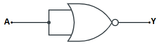
Ans: A is the input for the NOR gate and Y is the output.
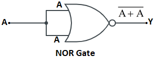
The output can be written as, $Y=\overline{A+A}=\overline{A}$
Truth table for the given combination:
Therefore, the circuit functions as NOT gate.
b)
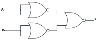
Ans: For the given circuit, A and B are the inputs and Y is the output.
From the result of the first case, we can conclude that the output of the first two NOT gates is $\overline{A}$ and $\overline{B}$.
The output for the combination can be written as:
$Y=\overline{\overline{A}+\overline{B}}$
$\Rightarrow Y=\overline{\overline{A}}.\overline{\overline{B}}=A.B$
Truth table for the given combination:
Therefore, the circuit acts as an AND gate.
NCERT Solutions for Class 12 Physics – Free PDF Download
Students will be benefited from NCERT Solutions for Class 12 Physics Chapter 14 Semiconductor Electronics. It provides the main concept of this chapter which enables students to get a clear idea on the chapter that increases the chances of scoring better in the examination. Class 12 Physics Chapter 14 contains mainly the idea of elemental semiconductor, introduction to p-n junction, Zener diode, semiconductor diode, digital electronics, logic gates, junction transistor etc. This chapter is so important that one can easily carry maximum marks in the board exams. Thus, NCERT Solutions for Class 12 Physics Chapter 14 Semiconductor Electronics enable them to do so. Diagrams, illustrations and graphs make this chapter interesting and understandable.
It will help students to perceive the chapter completely and also enable them to figure out the question by themselves. There are also miscellaneous questions which also help them to better understand this topic. Practicing with the help of NCERT Physics Class 12 semiconductors PDF which is given by Vedantu, students can easily crack all the problems and related questions in the examination hall. Semiconductor Electronics Class 12 NCERT Solutions are also available here and students can download it offline without any charges. Download the Chapter 14 Physics Class 12 NCERT PDF.
NCERT Solutions of Physics Class 12 Chapter 14: Semiconductor
Related Study Resources for Class 12 Physics Chapter 14 Semiconductor Electronics: Materials, Devices, and Simple Circuits
NCERT Exemplar for Class 12 Physics - Semiconductor Electronics - Free PDF Download
Previous Year Question Paper for CBSE Class 12 Physics (2020-2013)
Benefits of NCERT Solutions for Class 12 Physics
Some essential benefits that students could bring with the help of NCERT Solutions of semiconductor Class 12. The benefits are given below-
The given Class 12 Physics Chapter 14 NCERT Solutions are formulated properly based on its number division that follows the CBSE guidelines by professionals.
The Semiconductors Class 12 NCERT Solutions PDF are written in the easy simple aspect that every student can obtain prominently.
NCERT Solutions for Semiconductor Class 12 are easily accessible offline for future use, so students can easily practice it before the exam.
With the help of Vedantu’s app and NCERT Physics Class 12 semiconductors PDF, students can tackle all the questions which could trouble them in the exam. Without confusion, students can easily attain all the questions smartly and can improve their marks.
How Would Vedantu Study Material Help Students?
Vedantu's NCERT Solution for Chapter 14 Physics Class 12 is available for all subjects created by experienced teachers. They try to explain any topic step by step. Firstly, they briefly discussed the main context with the explanation with examples. Then, they gave all the important questions and answers that students easily cracked on the exam. Sentences are well constructed and grammatically strong and written simply.
In the Vedantu app, there is also a great opportunity to clear any topic related to doubts. Experts are always present there to help students to clear their queries. Download the Vedantu app to take the best guidance.
The key topics covered in this chapter include energy bands in conductors, semiconductors and insulators, semiconductor diodes- I-V- characteristics in reverse and forward bias, special purpose p-n junction diodes, diode as a rectifier, photodiode, LED, and solar cell. A few of the topics are also covered in the syllabus for CBSE Term 2 Class 12 Physics practical examination. So it is highly recommended that students must have a very clear understanding of each concept covered in Class 12 Ch-14 Semiconductor Electronics: Materials, Devices, and Simple Circuits to secure good marks in their 12th Boards Physics exam.
FAQs on NCERT Solutions for Class 12 Physics Chapter 14 Semiconductor Electronics: Materials, Devices, and Simple Circuits
1. What is an impure or extrinsic semiconductor? What is the difference between the extrinsic and intrinsic semiconductor?
When a small quantity of a specialized impure substance is mixed in a well-planned manner with pure and intrinsic conductors, then it is referred to as an extrinsic or impure semiconductor. The conductibility of the intrinsic semi is very poor, so increasing the conductivity of a semiconductor is the main purpose to do that. The process by which impurity is mixed is called doping and the next impure substance is known as a dopant.
2. Why should one choose Vedantu for CBSE Class 12 Physics notes?
There are so many reasons for choosing Vedantu as a guideline for the subject Physics as well as other subjects. These are available on Vedantu as PDF files containing Class 12 Physics Solutions. The solution is organized in such a systematic manner by which one can perceive the full knowledge and strengthen their concepts by reading those particular PDFs. So Vedantu is very supportive to make your lessons easier.
The expertise or teacher works their level best regularly to prepare their notes and all portions are covered by them so well that students will be able to get the best marks in their board exam. Chapter-wise model question answers are explained precisely with perfect clarification to offer the students the proper concept. Each mathematical problem is solved one by one without any step jump, which is easily acceptable for the students. Above mentioned features are much beneficial for students appearing on board exams.
3. What are the main advantages of using the NCERT Solutions for Chapter 14 Semiconductor Electronic: Material, Devices And Simple Circuits of Class 12 Physics?
The main advantage of using NCERT Solutions for Chapter 14 Semiconductor Electronic: Material, Devices And Simple Circuits of Class 12 Physics is that it aids the preparation and ensures that students are able to do well. Students can prepare short notes using the solutions to revise during the exams. The solutions are available in a simple and comprehensive way that can help students to prepare the chapter easily for the final board exams. The solutions can help students to memorize the questions quickly and score high marks in the board exams.
4. What is the best method to understand the concepts given in Chapter 14 Semiconductor Electronic: Material, Devices And Simple Circuits of Class 12 Physics?
Students can understand the concepts covered in Chapter 14 of NCERT Solutions for class 12 Physics by using the NCERT solutions for exam preparation. All concepts are explained properly and in sequence. Expert teachers at Vedantu have made it easy for the students to understand the concepts and get an in-depth knowledge of the concepts from NCERT Solutions. Students can refer to the solutions for final exams preparation and a quick revision during the exams. All the study material provided by Vedantu is also available on their mobile application and that too free of cost.
5. Are NCERT Solutions for Chapter 14 Semiconductor Electronic: Material, Devices And Simple Circuits of Class 12 Physics sufficient to prepare for competitive exams?
NCERT Solutions for Chapter 14 Semiconductor Electronic: Material, Devices And Simple Circuits of Class 12 Physics can help students to prepare for board exams as well as competitive exams. Solutions are explained in detail so that students can clear their doubts about the chapter easily. NCERT Solutions are given in a similar pattern based on the questions asked in the board exams and competitive exams. All solutions are given by professional and experienced physics teachers. They prepare the solutions after consulting different books and previous year papers to help students prepare well for their exams.
6. What are the different topics covered in Chapter 14 Semiconductor Electronic: Material, Devices And Simple Circuits of Class 12 Physics?
Class 12 Physics Chapter 14 is very important. It includes different topics that are important for the exam’s point of view. Students will study conductors, semiconductors, different types of conductors, p-n junction, semiconductor diode, Zener diode, application of junction diode as a rectifier, transistor, logic gates, and integrated circuits.
7. What is the most important advantage and disadvantage of semiconductor devices?
The most important benefit of semiconductor devices is that they are small in size so they require low voltage for working. The disadvantage of using a semiconductor device is that when high voltage and high temperature occurs, the semiconductor device can get damaged easily.